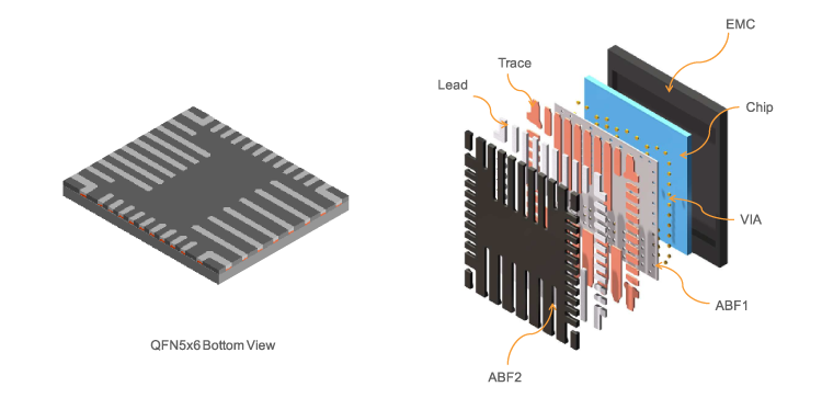
 structure of panel packaging products

 panel and products of siplp microelectronic

 advantages of siplp’s advanced packaging technology
●bumping/copper pillar middle process is not needed.
●thick trace can support bigger current.
●able to realize 6-side protection and the reliability reaches msl1. especially suitable for automobile electronics.
●thinner than fc (no substrate or lead frame)
●no bumping, unnecessary reflow, seamless connection, better product performance and higher reliability.
●smaller parasitic effect
●smaller on-resistance rdson
●flexible technology. especially suitable for mcm multiple chips packaging and power module packaging
●able to make copper clip pqfn and can realize double cooling.
●especially suitable for embedded passive device of power package, multiple chips package and module package.
●emi shielding anti-electromagnetic interference
●one panel one lot
●more suitable for the packaging of the third-generation semiconductors such as sic and gan.

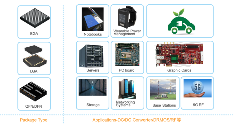
 siplp packaging way and main application fields
